
使用相同FLASH和管脚数量相同的芯片,例如GDF103C8T6移植STM32F103C8T6程序。虽然两个款芯片的寄存器地址以及架构基本相同。但是需要注意的是GD32F10x主频是108兆,但是STM32F10x主频是72兆。所以需要针对以RCC时钟进行修改。
例如打开原子哥的ALIENTEK MINISTM32 实验8 PWM输出实验例程。
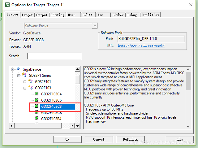
先将芯片的选项进行修改
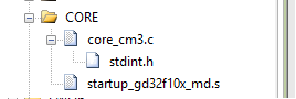
然后将STM32的启动文件替换成GD的启动文件
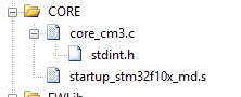
当然也可以不替换,我这里选择替换掉。
然后就想修改时钟相关配置
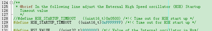
①打开stm32f10x.h文件,找到定义
//#define HSE_STARTUP_TIMEOUT ((uint16_t)0x0500) /*!< Time out for HSE start up /
修改为
#define HSE_STARTUP_TIMEOUT ((uint16_t)0xFFFF) /!< Time out for HSE start up */
这是因为GD频率高,并且稳定内部8兆的时钟HSE需要更多的时间,这里给满。
②修改system_stm32f10x.c文件
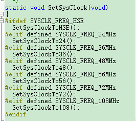
按照72MHz方式,添加108兆代码
1)
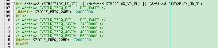
改为
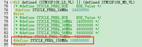
2)将
改为
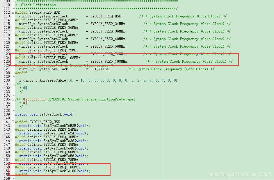
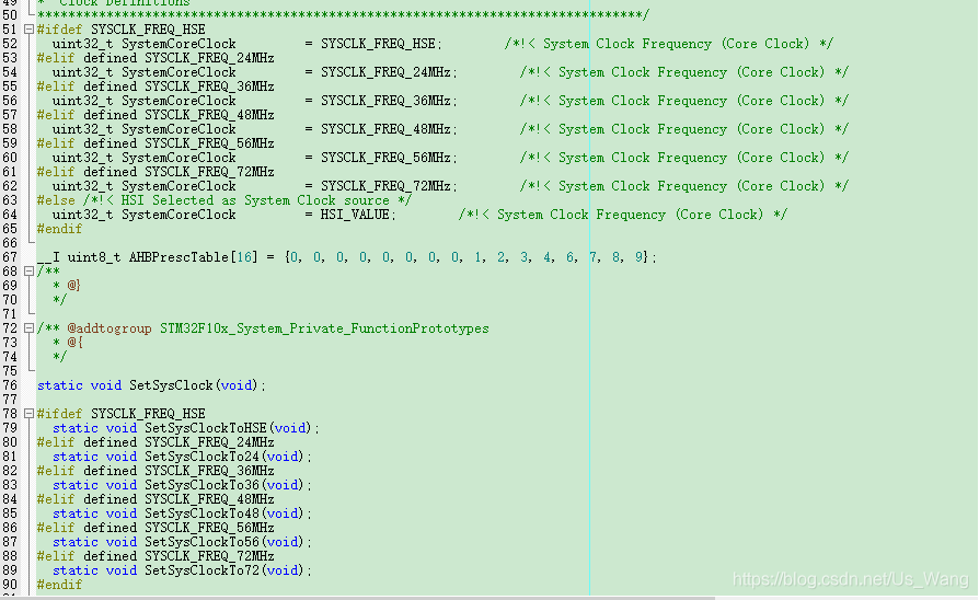
3)将
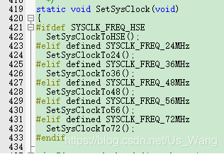
改为
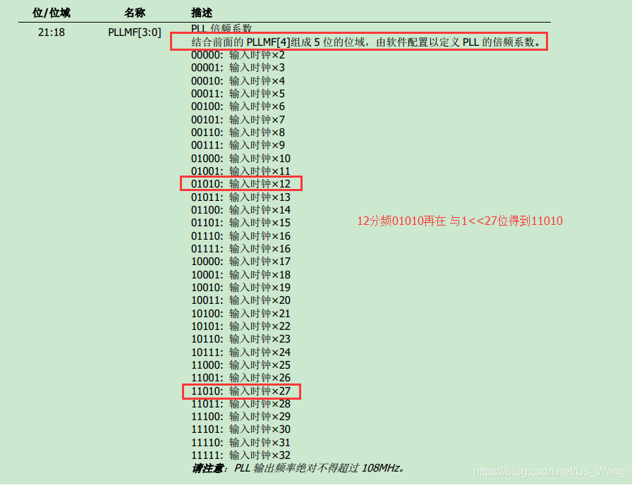
STM32的27位28位是保留的,但是GD的是用来配合PLL倍频的
在最后添加108兆的时钟配置程序
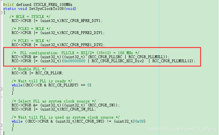
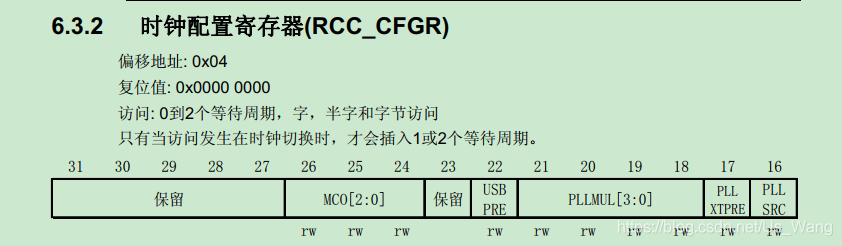
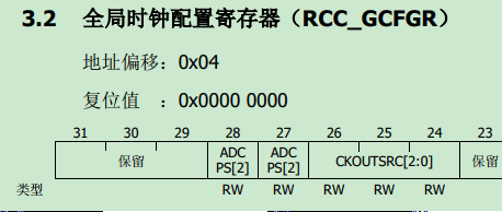
全局时钟配置寄存器在GD中命名时RCC_GCFGR,在STM32中命名为RCC_CFGR,关于PLL倍频系数配置PLLMF不同,红框内是先将HSE(8兆)分频为2得到4兆,然后27倍频得到108兆。
这时就得到了108兆的主频时钟
然后修改读取时钟的函数void RCC_GetClocksFreq(RCC_ClocksTypeDef* RCC_Clocks)
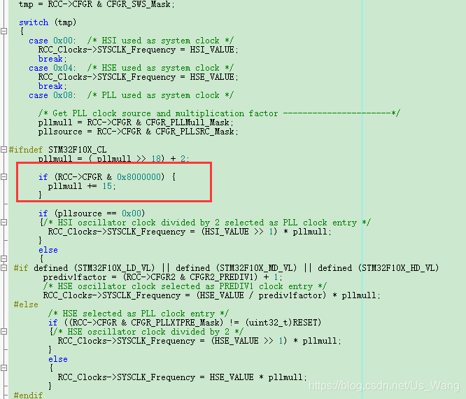
当发现时RCC_CFGR第27位置位了,就将倍频数从12+15 = 27.
至此,GD32F103移植ST32F103的工程就修改完成了,就可以尽情的使用ST的库代码了。
版权声明:本文为CSDN博主「嗯、我很帅」的原创文章,遵循CC 4.0 BY-SA版权协议,转载请附上原文出处链接及本声明。
原文链接:https://blog.csdn.net/Us_Wang/article/details/104472882